L01 Antenna design
-
Hello everybody!
I need to use the L01 OEM module for a prototype project which, in the end, if everything will go well will turn into a product. The project will mainly be focused on LoRa but I would like to include the BT and WiFi capabilities.
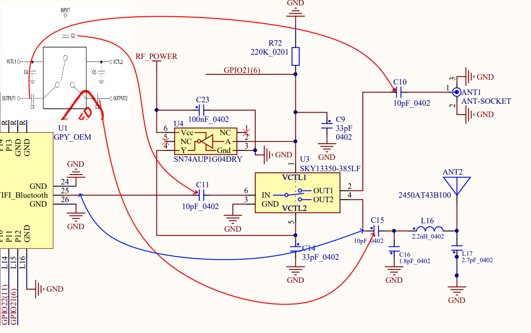
Since I have to design the PCB I will have to include the antenna. I don't have much experience with RF circuits since I've always used in my design complete modules with antennas already installed.For this project, I would like to use only a ceramic antenna so no antenna switch is needed. According to the circuit diagram of the "Universal OEM Baseboard" that uses the RF switch (SKY13350-382LF) the matching impedance circuit is made by L17, L16 and C16 - see picture attached. The other caps C9, C10, C11, C15,C 14 are used according to the RF switch datasheet.
My question is:
Will it be ok to just connect the output of the matching impedance circuit to the antenna pin of the OEM module (blue arrow)?
Thank you in advance for your answers.
-
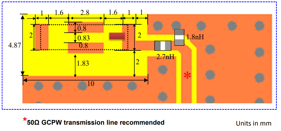
@Gijs Hi thank you for your reply. I intend to use the same antenna as the OEM module uses. According to 25450AT43B100 datasheet, the layout will be like the one below:
-
Hi,
I cannot make any guarentees for your final result, as there's some more to antenna design and placement than just the matching circuit.
You should be able to verify the matching circuit with the impedance of the ceramic antenna you're planning on using. If anything, I'd keep a capacitor in series at least, to block any DC coming in.